
Meet the MSP430 ADC Module
Now it’s time to start playing outside the “1” and “0” digital constructs, and dive into the analog world. The ADC10 module of the MSP430G2553 has a successive-approximation ADC, with 8 external channels (A0-A7). We’re not going to go into exact detail about how a successive-approximation ADC works, rather we will demonstrate the use of the module in a polling application, and an interrupt driven application. If you'd like to learn more about the successive-approximation ADC there's a pretty good wiki on the subject here.
There is a lot going on in the function block diagram of the ADC10 below, however, the only parameters we care about for this demo are the reference voltage, the input channel, the sample and hold timing, and the ADC10 timing. The ADC10 module has 8 registers that define its behavior. Of these registers only 3 will be needed : ADC10AE0, ADC10CTL0, and ADC10CTL1. These 3 registers control the voltage and timing parameters mentioned above. If you look over the family users guide for the MSP430G2553 you’ll learn that many of the values in the ADC10CTL0 and ADC10CTL1 cannot be altered unless the ENC bit is 0. Fortunately this is the default state, so we don’t need to start the ADC10 configuration clearing the ENC bit!

The basic steps for using the ADC10 module is to set the ADC channel, setup the clock for the device, and then start an ADC conversion. Now the conversion has two parts: sample and hold the channel voltage, and convert that sample to a digital value. The sample and hold part of the process can be set to sample the channel for 4, 8, 16, or even 64 sample and hold clock cycles. Once the voltage has been sampled a 10 bit binary value is generated representing the magnitude of the signal. The entire ADC10 conversion process can take as little as 17 clock cycles or as much as 77 clock cycles.

Before you start feeling overwhelmed by the ADC10’s options and configurations, just know that this module is primarily controlled by a small handful of registers. Of the 8 registers associated with the ADC10, we’re only going to focus on 3 in this tutorial—because those are the ones that actually determine how the module behaves. The others mostly support special cases like multiple-channel sequences or data transfers, which we won’t be covering here.
ADC10CTL0, ADC10 Control Register 0: This register controls most of the high-level behavior of the ADC. It’s where you choose your reference voltage (V+ and V−), enable interrupts, turn the ADC on or off, and select the sample-and-hold duration. It also contains the
ENCbit, which enables conversion, andADC10SC, which starts it.ADC10CTL1, ADC10 Control Register 1: This register selects which input channel to read from (A0 to A7), chooses the ADC clock source, and determines the conversion mode (single, repeat, etc.). This is where you also set the clock divider for slowing down fast clocks.
ADC10AE0, ADC Analog Enable Register 0: This register is what tells the MSP430 to treat a pin as an analog input instead of digital. To use a pin like P1.1 (A1), you need to set the corresponding bit in this register (i.e.,
ADC10AE0 |= BIT1).ADC10MEM, ADC Memory Register: This is where the result of a conversion ends up. After starting a conversion, you can read the 10-bit digital value from this register. If interrupts are used, this is the register the ISR reads.
ADC10DTCx (optional): There are also Data Transfer Control registers (
ADC10DTC0,ADC10SA, etc.) used when the ADC is configured for automatic data transfers across multiple channels. These are more advanced features and won’t be used in this tutorial.
According to the MSP430 Family User Guide, many of the configuration bits in the ADC10 control registers are locked while a conversion is enabled (ENC = 1). Fortunately, the ENC bit is cleared by default, which means you're free to set up the module as needed before kicking off any conversions. Just be sure not to set the ENC bit until your configuration is complete.
The diagram below shows which pins can serve as analog inputs on the MSP430G2553 20-pin package. If you’re using an input like A1 (P1.1), be sure to configure that pin properly in ADC10AE0, and avoid using it for digital I/O at the same time.

ADC-Based PWM Code and Program Flow
What This Code Does!
This example reads an analog voltage from pin P1.1 (A1) using the MSP430’s ADC10 module. That voltage is continuously converted into a 10-bit digital value, which is then used to control the duty cycle of a PWM signal on P2.1. The higher the input voltage, the wider the pulse—allowing something like an LED to appear brighter in proportion to the analog input.
The PWM signal is generated using Timer A, but instead of hardcoding a duty cycle or using manual input like a button, we let the analog signal do the talking. The ADC operates in interrupt-driven mode: once a conversion completes, the result is read and the next conversion is automatically started. This allows for smooth, ongoing analog control with minimal CPU involvement.
Equipment You Need
MSP-EXP430G2ET Development Kit
MSP430G2553
10k potentiometer
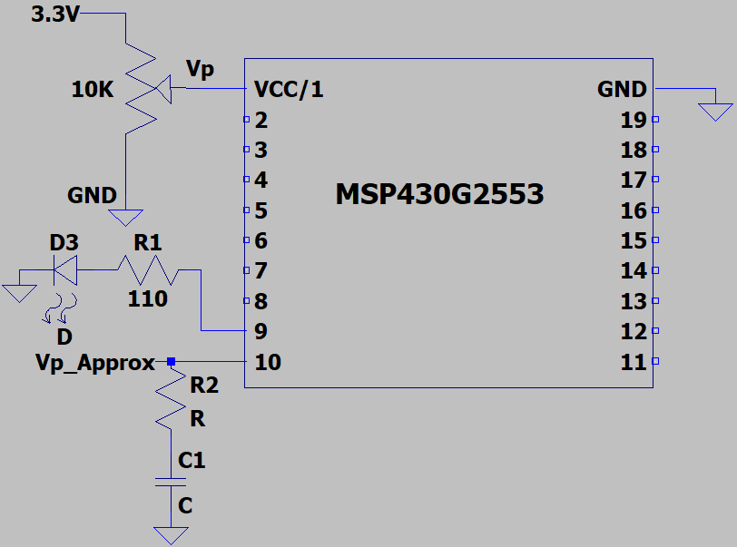
Below is a schematic illustrating the components used in this code and their connections. D3 is located on the Launchpad board (MSP-EXP430GET Kit), so the only additional part that you will need is the 10k potentiometer and some wires to make the connections.

The FLOW
The program flow for this project is structured into 4 key parts. While similar in format to the previous tutorials, this project introduces the MSP430's ADC10 module, which will monitor an analog voltage on P1.1. That voltage will be digitized and used to dynamically control the duty cycle of a PWM signal output on P2.1. The conversion will be handled via interrupts for efficient operation.
MSP430 library declaration and program definitions
This section includes the necessary header (
<msp430.h>) and any preprocessor macros or global variable declarations used throughout the code—for instance, defining which bit corresponds to the analog input pin.Function Prototypes
Although this example may not use any user-defined functions, this section is included for consistency and future expandability. If helper functions are created, their prototypes should go here.
Main Routine
Turn off Watchdog Timer
Prevents the MSP430 from resetting unexpectedly during development by disabling the watchdog timer right at startup.
Set the clock speed
Loads calibration constants to configure the digitally controlled oscillator (DCO) for the desired operating frequency (e.g., 16 MHz). This ensures that both Timer A and the ADC module operate with consistent timing.
Setup the Modules Being Used
Configures the ADC10 module: selects the input channel, sets the reference voltage, sample-and-hold duration, and enables analog input on the correct pin. Timer A is also configured to generate a PWM signal on P2.1, with a duty cycle driven by the ADC value.
Enter "Forever" Loop
The CPU enters low-power mode with interrupts enabled (
__bis_SR_register(LPM0_bits + GIE)), effectively handing control over to the ADC ISR. The main loop doesn't actively do anything—it just waits for the ADC to complete a conversion and adjust the PWM output accordingly.
ISR(s) or Function Definitions
ADC10 Interrupt Service Routine
This ISR is triggered when an ADC conversion completes. It reads the result from
ADC10MEMand updates the duty cycle register (TA1CCR1) to match. It also restarts the next conversion cycle by re-enabling and re-triggering the ADC
The ADC-Based PWM Code
When coping the code below some times the #include <msp430.h> header (line 2) doesn't get copied correctly. Simply copy line 2 into your code and build, then run, and you should be adjusting LED brightness with the best of them.
Turning A PWM Signal Into a "Ghetto" DAC
By enabling the Timer A output on P2.2 and throwing the corresponding PWM signal into a resistor capacitors series combination, we will be able to turn our PWM signal into a ruff DC equivalent of the DC signal on the potentiometer. Of course it's not exactly the same, in fact, if you place a scope across the capacitor you'll see a charging and discharging of the cap voltage, which can approximate our potentiometer voltage, but it's certainly not an exact replica of it.
To Enable the Timer A output on P2.2 add the following lines of code just below line 29:
P2DIR |= BIT2;
P2SEL |= BIT2;
In addition to the above code, you have to attach the RC circuit as shown in the figure below, and then you'll have a rough DAC of the DC signal on the potentiometer.
All Tutorials Must End
When I first started working with the ADC10 module, I found it a bit intimidating — not because it was overly complex, but because it felt like there were a lot of moving parts to get just right: references, channels, sample timing, interrupts. But as you’ve seen, once you break it down and try it in a real application, it becomes much more approachable.
This example gives you a solid starting point for analog input on the MSP430 using interrupts. Like the Timer tutorial, this isn’t an exhaustive guide, but more of a practical cookbook to get your hands dirty. If you’re stuck, feel free to shoot me a message and I’ll do what I can.
Good luck and cheers!