
Meet the MSP430 Ports
Every MSP430 has port modules, and those port modules are controlled, and configured by 9 different registers – that’s right, 9! Now that might seem like a lot of overhead for controlling some digital IO, but we’ll break it down so it’s not so overwhelming. The function of the port modules are controlling pin function. The port modules dictate weather a pin is a digital output, digital input, if a given input is interrupt capable, and provides access to the pin for other modules like the ADC module, or the Timer A Module.
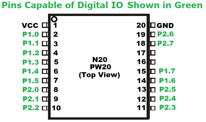
Before we give a list of these 9 port registers one needs to see just what these ports control! Above is a figure that shows the pins that the port module actually controls on the MSP430G2553 chips. This device only contains two ports: Port 1, and Port 2. Every pin of these two ports can be either an input or an output, and each pin can trigger an interrupt.
Alright, now that we have a more precise understanding of what these port registers control (namely pin function) lets give names to these registers and a brief description. Keep in mind, each register is 8 bits in length and each bit is a representation of its corresponding pin. The x denotes 1 or 2, for Ports 1 and 2, so that PxIN can be P1IN or P2IN.
PxIN register, represents the value on a given pin when it’s setup as an input, so you would check this register to see if a given input is High or low.
PxOUT register, represents the output value on the port pins setup as output. If you write a 0x01 (1 in Hex) to the P1OUT register then pin P1.0 will get set high, provided that pin is set to output. If it’s set to input then the PxOUT port sets the input pin up with pullup (if set high), or pulldown (if set low), resistors on the input. Of course, the pullup/pulldown functionality is enabled with another Register (PxREN).
PxDIR register, this configures the direction of the pin as input or output. A high sets the associated pin as an output, and a low sets it as input.
PxREN register, enables the pullup/pulldown function of an input. The PxOUT register controlled if the input is either pulled up or pulled down, as mentioned above.
PxSEL & PxSEL2 registers, the pins of the MSP430 are multiplexed with up to four different modules and these registers allow you to select which module is being utilized by the pin. We’ll get into specifics later, but for now know that for a given pin if it’s PxSEL and PxSEL2 register is set to low then said pin will function as a digital IO pin.
PxIE register, enables Port 1, or 2, pins for interrupts.
PxIFG register, indicates which pin input triggered an interruption on Port 1 or 2.
PxIES register, sets the associative pin for either a positive edge triggered (high), or negative edge triggered (low), interrupt configuration for Port 1 or 2.
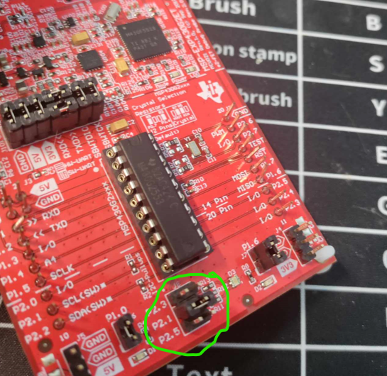
P2.1 Jumper Connection
This tutorial won't work if you don't have P2.1 connected to the D3 diode using a jumper, as shown in the picture below.
program Flow and PWM code (Output Only)
Okay so now we know the names of the registers we will be playing with, but before we dive into programming let’s talk about program flow. Generally, our program will consist of an MSP430 library declaration and any program definitions used, Function Prototypes (for any subroutines made), the Main program routine, and finally any ISR and Function definitions that are used. The Main routine itself will first disable the watchdog timer, set the clocking speed of the CPU, then setup the modules needed for the program, and its “forever” loop will be entered into. Now this “forever” loop can be event driven by various interrupts, or it can simply be an infinite while loop blinking an LED. In summary, all MSP430 tutorial programs will have the following format:
MSP430 library declaration and program definitions
Function Prototypes
Main Routine
Turn off Watchdog Timer
Set the clock speed
Setup the modules being used
Enter "forever" loop
ISR’s or Function Definitions if used
This will be illustrated with our first program. It’s nothing fancy. We’re just going to control the brightness of the red LED on pin 2.1 (P2.1), using pulse width modulation (PWM). Our first program will only use P2.1 as an output. It won’t use any subroutines or interrupts, so items 2 and 4 in the above list can be neglected. However, with this first example we will walk you through how to create your first project in Code Composer, write the program, and load it onto the MSP430.
Start Code Composer, and then select File -> CCS Project, from the main menu tab.

The New CCS Project wizard should pop up as shown below. Choose MSP430G2553 as the target, name the project name whatever you want (I chose myPWM) in the Project Name box, select “Empty Project (with main.c)” as a template, and press finish.

After you press Finish in the last step Code Composer will generate your project with a main.c template file. The template given completes Step 3.i of the program format we will be adhering to, but we need to work a bit on Step 1 because our program will use a couple definitions, and Steps 3.ii through 3.iv need a bit of work. This program won’t have any function prototypes, subroutines, or ISRs so those section will be left blank. Below is the main program that Code Composer should have given you, minus some comments made to help tie this exercise to TDP's MSP430 program format.

Now we’re going to add some definitions: DutyCycle_Ref, and Period_Ref. These definitions will correspond to the duty cycle and period, of our signal.

Now we are going to configure the clock system of the MSP430, which is done in Step 3.ii. The clocking system can be pretty involved, but our goal here is just to demonstrate how to set the clock. Luckily, the MSP430 comes with some preset calibration labels. These labels can be found on page 15 of the MSP430G2553 datasheet along with more information on the Clock Module.

These labels are just instructions to two clock module registers: Basic Clock System Control 1 (BCSCTL1), and DCO Control (DCOCTL). In the image above you can see that we're loading the 1MHz calibration label into BCSCTL1, and the 1MHz calibration label into the DCOCTL register. There are total of 4 Calibration Label frequencies: 1MHz, 8MHz, 12MHz, and 16MHz. Of course, clocking module is capable of producing other frequencies.
Moving onto Step 3.iii, we will be setting up the Port Modules. Namely we have to set the direction of the pin we intend to use (P2.1) to output. Upon start up the MSP430 port pins are set to input as default, but before we set the direction of P2.1 to output, we will ensure that it starts it's output in a known state - low. We do this with a bitwise clear of the 2nd bit of the P2OUT register, or Bit1 - this is a bit redundant since the P2OUT register starts up cleared as default.
The P2OUT &= ~BIT1 instruction only clears the BIT1 bit, and leaves the others untouched. After this instruction we do a Bitwise OR on Bit1, which only sets Bit1 turning p2.1 to an output set to low by the previous bitwise clear command.
Here we create our forever loop. The first thing that is done is that an int variable is made called period, and it's initiated with zero, and immediately after we set P2.1 high, and then we enter into our forever loop.

The forever loop above checks for 4 conditions all of which are stipulated in those if statements. The first if statement checks to see if the PWM is set to be always on, in which case, the duty cycle is at 100% and our LED is always on, regardless of the period value. The next if statement handles the case where the period equals the DutyCycle_Ref or the DutyCycle_Ref equals zero, in both cases our LED is turned off. Now we get to the last case where the period variable equals the Period_Ref definition value, and this is ANDed with the defined DutyCycle_Ref number because we don't want our state machine turning on the LED when the reference value is set to 0.
When running this code make sure the Period_Ref number is positive and larger than the DutyCycle_Ref and the DutyCycle_Ref must be positive, otherwise this state machine won't do anything interesting! However, as long as those requirements are met feel free to play around with values.
Below is a picture of the PWM Duty cycle equal to 10% (DutyCycle_Ref = 25), 50%(DutyCycle_Ref = 127), and 100% (DutyCycle_Ref = 255). As you can see the LED is gets brighter with increased duty cycle - no shocker there.

Below is the PWM code. You can download and play with the duty cycle values yourself. It's pretty straight forward code.
The program we just made creates a PWM signal on pin 2.1,but the modulation is fixed on startup because it uses the static defines (DutyCycle_Ref and Period_Ref) to control the duty cycle and period of the PWM. For a more “useful” PWM we’re going to make the duty cycle variable so we can change it while the program is running. We will do this by making a volatile variable called duty and place it just before the main function call. The volatile keyword tells the compiler that the variable can be affected by things outside the scope of the program (like a button push) and it tells the compiler not to optimize it away. This variable will be controlled in an ISR that will be controlled by the button attached to P1.3. However, before we just throw interrupt code at you, we’ll go over how interrupts are handled in C.
Handling an interrupt in an MSP430 is a somewhat cumbersome affair. If the Processing unit receives, and accepts an interrupt, the status register and program counter are saved, the MSP430 determines where the interrupt came from and jumps to that interrupt vector. Now, the interrupt vector that it jumps to may, or may not, have code associated with it. The #pragma keyword tells the compiler which ISR vector the following code is associated with, and the __interrupt void function Name(void) tells it to save the context (i.e. the status register, and PC) of the system. In addition, once the code between the brackets is completed, the MSP430 returns to where it was in the main program before it received the interrupt.

The MSP430G2553.h file has definitions for the Interrupt vectors, as shown below. You can find all the interrupt vectors for the device and the priority of the interrupts on the MSP430G2553 datasheet on page 11. Here we're going to use the interrupt vector for port 1 defined as PORT1_VECTOR. This tells the compiler that the code that follows is to be associated with that VECTOR and thus that interrupt. The above PORT1_VECTOR ISR routine is blank, but we ill fill it in later with code.

So far we've described how the MSP430 handles an interrupt request, and shown how to associate code with the ISR, but we haven't said how to get a given pin setup for interrupts. This basically takes 5 lines of code. The first 3 set the pin up for an input, either pulled up or down, and the last two set which edge the interrupt will trigger on (positive edge, or negative edge) and, finally, enable the pin as an interrupt.
1. P1DIR &= ~BIT3; //Set P1.3 as input
2. P1OUT |= BIT3; //Set Pullup Resistor
3. P1REN |= BIT3; //Enable pullup Resistor
4. P1IES |= ~BIT3; //Set Interrupt to trigger on low to high edge
5.P1IE |= BIT3; //Set Interrupt enable.
Ok, so we've explained how to associate code with an interrupt vector, and the five lines of code you need to setup a pin to produce an interrupt. The only bit we haven't explained is how to enable interrupts on the MSP430, this is done simply enough with one line of code:
__bis_SR_register(GIE);
This line enables the interrupts in the MSP430 status register and should be placed somewhere before our forever loop, so our system will actually respond to interrupts.
Input Driven Interrupt using P1.3
For this next exercise, we're going to alter our previous PWM code so that the duty cycle can be altered in software by pressing the switch attached to P1.3. The button will toggle the duty cycle to one of 6 states
State 0: 10% duty cycle
State 1: 30% duty cycle
State 2: 50% duty cycle
State 3: 80 % duty cycle
State 4: 100% duty cycle
State 5: 0% duty cycle
To this we need to add a volatile variable (to hold the duty cycle), change P1.3 to an interrupt cable input, enable general interrupts, modify sate machine to use the new Duty volatile variable, and write an ISR associated with the PORT1 interrupt. Without further delay, lets get started.
The first alteration we need to do to the PWM code is to add a volatile variable. You can see this declaration on line 16 in the image below. It's initialized at 127, which is a 10% duty cycle.

We add five lines of code (lines 37, 38, 39, 41, and 42), as stated previously, to setup P1.3 as an input capable of interrupts.

Next, we have to enable interrupts with the "__bis_SR_register(GIE)" instruction. In addition, the state machine of our program needs to be changed to reflect the new Duty variable. This is easily done by replacing every instance of DutyCycle_Ref with Duty in our while loop. There are only 4 instances. The instances where Duty was used to replace DutyCycle_Ref are shown below.

The final piece of code that needs to be added is the ISR. On line 81 (after the main function) you can see we used the #pragma vector=PORT1_VECTOR to tell the compiler that this function is an interrupt and to give it the correct memory vector. The "__interrupt void myISR(void){," line is then used to tell the compiler to save the context of the current microprocessor state, and then branch off to the vector to start the ISR code.
Line 83 clears the interrupt of the pin, so we don't reenter out interrupt code.
Lines 85-98 consist of a switch statement, which looks at the current value of Duty and goes to next highest Duty cycle value, unless it's all ready at 100%, in which case, it goes to 0% Duty.
Finally, once you compile and upload the new program to the MSP430, you should be able to cycle through all the Duty cycles as shown below.

Here's final .
Port Selection Registers
We’ve used almost every register in the port module except we haven’t used the PxSEL, and PxSEL2 registers. These registers are used to give access to the other modules in the MPS430. The default status for pin function is to operate as digital IO, which is why we didn’t have to alter the PxSEL and PxSEL2 registers. When using TimerA, the ADC, or the USCI modules, one has to alter the port select registers (PxSEL, and PxSEL2).
The picture below shows the pins with their associated function selections. Pin 2 for example can be a digital IO (P1.0), or it can function as a clock input to the TimerA module (TA0CLK), or as a system clock input (ACLK), or as an ADC input(A0), or as an input to the comparator module (CA0). We haven’t mentioned the comparator module and I’m not sure if we will be making a tutorial about it but may be. The various port functions are accessed using the port select registers, and the direction port (PxDIR). In addition, further setup might be needed depending on the module being accessed via the port. We will cover port selection in more detail in later tutorials.

Well, that's it for this round. Good luck on your endeavors!