
Understanding the ZYBO Architecture
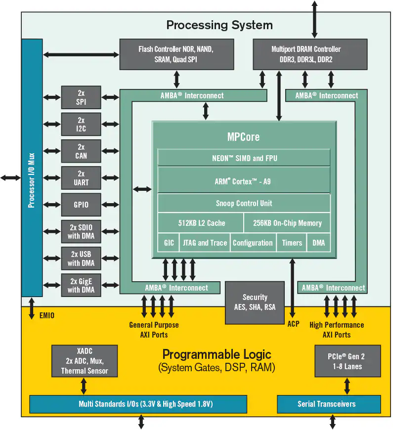
Before we start building Linux systems and FPGA designs, it's worth spending a few minutes understanding what is actually on the ZYBO board.
The ZYBO is built around a Xilinx Zynq-7000 device. What makes the Zynq family interesting is that it combines two very different technologies into a single chip:
A dual-core ARM processor system
An FPGA fabric
Think of it as a Linux computer and an FPGA living inside the same package.
The Processing System (PS)
The Processing System, usually abbreviated PS, contains the ARM processors and the hardware needed to run an operating system.
Some of the major components include:
Dual-core ARM Cortex-A9 processors
DDR memory controller
Ethernet controller
USB controller
SD card interface
UART interfaces
Timers and interrupt controllers
When we boot PetaLinux, the operating system runs entirely on the ARM processors inside the Processing System.
You can think of the PS as a small embedded computer. It provides the processing resources required to run Linux and the applications that execute within it. Throughout this tutorial series, Linux running on the PS will be responsible for configuring hardware, managing peripherals, and providing the software interface to our FPGA designs.
For many embedded applications, the Processing System alone provides all of the functionality required.
The Programmable Logic (PL)
The Programmable Logic (PL) is the FPGA portion of the Zynq device.
This is where we create custom hardware using VHDL or Verilog. Unlike software, which executes instructions one at a time, hardware in the FPGA operates in parallel. Multiple hardware modules can execute simultaneously on every clock cycle.
Typical FPGA designs include signal generators, digital filters, PWM generators, communication interfaces, custom peripherals, and high-speed data acquisition systems.
This parallel architecture makes the FPGA extremely powerful for applications requiring deterministic timing or high-performance data processing.
Why Combine a Processor and an FPGA?
Traditionally, embedded systems requiring both software and custom hardware often used two separate devices: a microprocessor to execute software and an FPGA to implement specialized hardware.
The Zynq combines both into a single System-on-Chip (SoC), allowing the ARM processors and FPGA fabric to work together much more closely.
For example, Linux can configure registers inside an FPGA peripheral, hardware implemented in the FPGA can notify Linux when a task has completed, and computationally intensive algorithms can be accelerated in hardware while the processor handles the higher-level application logic.
This close integration is one of the reasons the Zynq family has become so popular in embedded systems.
Communication Between the PS and PL
One of the features that makes the Zynq architecture so powerful is the variety of communication paths available between the Processing System and the Programmable Logic. As shown in the figure below, the boundary between the PS and PL contains several interfaces, each designed for a different purpose.
While we won't explore every interface in detail just yet, understanding their general purpose will make the rest of this tutorial series much easier to follow.
AXI General Purpose (GP) Interfaces
The General Purpose (GP) AXI interfaces are primarily used for controlling hardware implemented in the FPGA fabric. Software running on the ARM processors can read from and write to registers exposed by custom peripherals, allowing Linux applications to configure hardware, change operating parameters, or retrieve status information.
Throughout this tutorial series, these interfaces will become our primary method for connecting Linux applications to custom FPGA hardware.
AXI High Performance (HP) Interfaces
The High Performance (HP) AXI interfaces are optimized for moving large amounts of data between the Processing System and the Programmable Logic.
Applications such as image processing, high-speed data acquisition, or digital signal processing often rely on these interfaces to efficiently transfer data between FPGA hardware and DDR memory.
Accelerator Coherency Port (ACP)
The Accelerator Coherency Port (ACP) provides a specialized communication path that allows hardware in the FPGA fabric to access memory while remaining coherent with the ARM processor caches.
Although ACP is an important feature for hardware accelerators, it is generally used in more advanced applications than those covered in this introductory series.
Extended Multiplexed I/O (EMIO)
Not all communication involves moving data. The Extended Multiplexed I/O (EMIO) interface allows signals associated with Processing System peripherals to be routed through the FPGA fabric.
This makes it possible for FPGA logic to interact directly with GPIO and other peripheral signals or to customize how those signals are routed within the design.
Interrupts
Communication is not limited to software controlling hardware. Hardware implemented in the FPGA can also notify the ARM processors when an event has occurred by generating an interrupt.
For example, a custom peripheral might generate an interrupt when a measurement completes, new data becomes available, or an error condition is detected. Rather than continuously polling the hardware, Linux can simply wait for the interrupt and respond when one occurs.
Putting It All Together
The Zynq provides several communication mechanisms because different applications have different requirements. The GP interfaces are ideal for configuring hardware, the HP interfaces are optimized for high-speed data movement, the ACP supports cache-coherent memory access, EMIO routes peripheral signals through the FPGA fabric, and interrupts allow hardware to notify software when attention is required.
As we work through this tutorial series, we will primarily focus on the AXI General Purpose interfaces, since they provide the simplest and most common way for Linux applications to interact with custom FPGA hardware. The remaining interfaces will be introduced in future projects as they become relevant.
The Development Workflow
When working with a ZYBO project, the tools generally have the following responsibilities:
Vivado
Vivado is used to design the hardware system. Here we configure the Zynq Processing System, add custom IP, connect AXI interfaces, and generate the FPGA bitstream along with the hardware description exported as an .xsa file.
PetaLinux
PetaLinux takes the hardware platform created by Vivado and builds a bootable embedded Linux system. This includes the Linux kernel, device tree, root filesystem, bootloader, and boot images required to run Linux on the ARM processors.
Vitis
Vitis is used to develop software that executes on the ARM processors. Depending on the project, this may include bare-metal applications, Linux applications, or software used to communicate with custom FPGA hardware.
What We Will Build
Throughout this tutorial series, we will combine the flexibility of Linux running on the ARM processors with the performance of custom hardware implemented in the FPGA fabric.
Our projects will gradually introduce custom peripherals, Linux drivers, AXI interfaces, and hardware accelerators while demonstrating how software and hardware work together to build complete embedded systems.
Understanding the relationship between the Processing System and the Programmable Logic is the foundation for every Zynq project. Once that relationship becomes clear, the rest of the development workflow begins to fit together naturally.